
From napkin to PCB: designing SolveBlock in KiCad
How a speedcubing idea became a custom ESP32 board — the requirements, the schematic decisions, the layout tradeoffs and the mistakes I'd happily make again.
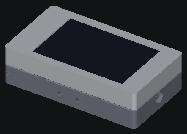
SolveBlock started the way good products usually do: with a real person who had a real annoyance. Speedcubers time their solves on dedicated timers, and those timers are excellent at exactly one thing — timing. Everything around the timing (sessions, averages, history, a nice display) lives somewhere else, usually a phone propped against a water bottle.
We wanted one dedicated device that sits next to the timer and does the rest. This is how it went from a sketch to a board.
Start with requirements, not parts
The temptation is to open KiCad first. Don't. I wrote a one-page requirements list before choosing a single component:
- The external timer stays the source of truth. We read its time; we never re-time a solve ourselves.
- Show the current solve, session stats and averages on a clear display.
- Input that stays out of the way — ideally none at all for a normal solve, since the cuber's hands just let go of a cube.
- Genuinely offline: no Wi-Fi, no Bluetooth, no account, nothing to log into.
- Fit a printed enclosure that sits beside the timer and doesn't slide.
That first requirement shaped almost everything else, and it's worth its own post.
A note on tools: I design in KiCad. It's free, open source and more than capable for a board like this. Altium Designer is the commercial standard in a lot of companies and worth knowing if you're heading that way professionally, but for a small team shipping a first product, KiCad does everything needed — schematic, layout, 3D view and fabrication outputs.
Picking the parts
An ESP32-class board was the obvious brain: enough RAM for a display buffer, plenty of GPIO, and a toolchain we already knew. Its radio is never used — requirement 4 says the device is offline, and "no Wi-Fi, no Bluetooth" is a stronger promise than "works offline". Starting from an existing display board rather than a bare chip meant the hard layout (flash, crystal, display interface) was already done. That's not where a small team should spend its first revision.
The rest of the block diagram:
- Display on SPI, chosen for readability across a table more than for resolution.
- Input: a touchscreen, so nothing sits under the cuber's hands. A normal solve costs zero input — the timer's own reset signal doubles as "keep and next" — so the screen only gets touched for a +2, a DNF or a discard.
- Timer interface: a connector and a small signal-conditioning stage so the timer's data line arrives at a level the ESP32 is happy with.
- Power: USB in, a clean 3.3 V rail and bulk capacitance close to the processor and display.
Schematic habits that saved me
- Respect the strapping pins. On the classic ESP32, GPIO0, 2, 5, 12 and 15 affect boot behavior. GPIO12 in particular sets the flash voltage at boot, and an accidental pull-up there can leave a board that won't start. I kept user-facing signals off those pins.
- Remember the input-only pins. GPIO34–39 have no output driver and no internal pull-ups. Good for buttons with external resistors; useless for chip selects.
- Add test points everywhere. 3.3 V, ground, TX/RX, EN and the timer data line all got a pad. Bring-up is so much easier when you can clip a probe on something.
- Expose a boot/reset path. Auto-reset through the USB-serial chip, plus physical pads for EN and GPIO0 in case the automation fails.
Layout: the part where the real tradeoffs live
The first placement wasn't decided by electronics at all. It was decided by the enclosure: where the display window sits, where the cable exits, where a thumb lands. I exported the board outline, built the enclosure around it in OpenSCAD, printed it, then moved parts and did it again. PCB and plastic evolved together.
Some electrical rules I wouldn't skip:
- Use a solid ground pour, stitched with vias, and keep return paths short.
- Put decoupling capacitors right at the power pins, not "somewhere nearby."
- Route the display's SPI clock away from the timer data line — the one signal this device must never misread.
Revision one isn't supposed to be perfect
A first board will always teach you something: a connector footprint that's mirrored, a control that's awkward once the lid goes on, a part that's hard to hand-solder. That's fine, because Rev A is meant to teach. The goal of a first board isn't to be right; it's to be measurable. If every likely problem has a test point or a log line that makes it obvious, the lessons are cheap.
What I'd tell anyone starting their first board
- Write the requirements first and pin them above your monitor.
- Use modules for anything RF.
- Design the board and the enclosure together.
- Budget for at least two revisions, emotionally and financially.
SolveBlock has gone through several PCB and enclosure revisions since, and every one of them started by re-reading that one-page list.
Update: the board this note describes became SolveBlock Core Rev C, a custom ESP32-S3 PCB.
Some links in these notes are affiliate links. If you buy through one, I may earn a commission at no extra cost to you. I only link to tools I use or would recommend.